Monday, April 18, 2011

Simple model of ADC, noises in ADC and ADC non-linearity

An analogue-to-digital converter transforms a continuous quantity (voltage or current) into a discrete time digital numbers proportionally to the magnitude of the voltage or current. Most ADCs convert an input voltage to a digital word, but the definition of an ADC includes the possibility of an input current.

An ADC has an analogue reference voltage $V_{REF}$ or current against which the analogue input is compared. The digital output tells us what fraction of the reference voltage or current is the input voltage or current. So if we have N-bit ADC, there are $2^N$ possible output codes, and the difference between each output code is $\frac{V_{REF}}{2^N}$.

Resolution of ADC
Every time you increase the input voltage by $V_{REF}/2^N$ Volt, the output code will increase by one bit. This means that the least significant bit (LSB) represents $V_{REF}/2^N$ Volt, which is the smallest increment that the ADC actually can \textit{resolve}. Then one can say that the \textit{resolution} of this converter is $V_{REF}/2^N$ because ADC resolve voltages as small as such value. Resolution may also be stated in bits.

Because the resolution is $V_{REF}/2^N$, better accuracy / lower error can be achieved as: 1) use a higher resolution ADC and/or 2) use a smaller reference voltage. The problem with high-resolution ADC is the cost. Moreover, the higher resolution / lower $V_{REF}/2^N$, the more difficult to detect a small signal as it becomes lost in the noise thus reducing SNR performance of the ADC. The problem with reducing $V_{REF}$ is a loss of input dynamic range.

Hence the ADC's resolution indicates the number of discrete values that can be produced over the range of analogueue values and can be expressed as:
$$ K_{ADC} = (V_ \mathrm {REF} - V_ \mathrm {min})/N_{max}$$

where $V_ \mathrm {REF}$ is maximum (reference) voltage that can be quantified, $V_ \mathrm {min}$ is minimum quantifiable voltage, and $N_{max} = 2^M$ is the number of voltage intervals ($M$ is ADC's resolution in bits). The ADC's output code can be represented as:

$$ADC_ \mathrm {Code} = \textrm{round}\left[ (V_ \mathrm {input}-V_ \mathrm {min})/K_{ADC} \right]$$

The lower reference voltage $V_{REF}$, the smaller range of voltages with greater accuracy one can measure. This is a common way to get better precision from an ADC without buying a more expensive ADC with higher resolution.


Quantisation error
As the input voltage in ADC increases towards $V_{REF}/2^N$, the output still remains at zero because a range of input voltages is represented by a single output code. When the input reaches $V_{REF}/2^N$, the output code changes from 000 to 001.

The maximum error in ADC is 1 LSB. This 0 to 1 LSB range is known as the ``quantisation
uncertainty'': there is a range of analogue input values that could have caused any given code.


Linearity and Linearity errors
The accuracy of analogue to digital conversion has an impact on overall system quality and efficiency. To be able to improve accuracy you need to understand the errors associated with the
ADC and the parameters affecting them.


Differential Linearity Error

Differential Linearity Error (DLE) describes the error in step size of an ADC: it is the maximum deviation between actual steps and the ideal steps (code width). Here ``ideal steps''' are not for the ideal transfer curve but for the resolution of the ADC. The input code width is the range of input values that produces the same digital output code.

Ideally analogue input voltage change of 1 LSB should cause a change in the digital code. If an analogue input voltage greater than 1 LSB is required for a change in digital code, then the ADC has the differential linearity error.
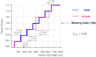


Here each input step should be precisely 1/8 of reference voltage. The first code transition from 000 to 001 is caused by an input change of 1 LSB as it should be. The second transition, from 001 to 010, has an input change that is 1.2 LSB, so is too large by 0.2 LSB. The input change for the third transition is exactly the right size. The digital output remains
constant when the input voltage changes from 4 LSB to 5 LSB, therefore the code 101
can never appear at the output.

When no value of input voltage will produce a given output code, that code is missing from the ADC transfer function. In data sheets of many ADC it is specified ``no missing codes''; this can be critical in some applications like servo systems.


Integral Linearity Error
Integral Linearity Error (ILE) describes the maximum deviation of ADC transfer function from a linear transfer curve (i.e. between two points along the input-output transfer curve). It is a measure of the straightness of the transfer function and can be greater than the differential non-linearity. In specifications, an ADC is described sometimes as being ``x bits linear.''
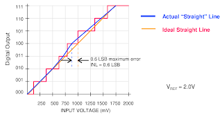

The ADC input is usually connected to an operational amplifier, maybe a summing or a differential amplifier which are linear circuits and process an analogue signal. As the ADC is included in the signal chain, we would like the same linearity to be maintained at the ADC level as well. However, inherent technological limitations make the ADC non-linear to some extent and this is where the ILE comes into play.

For each voltage in the ADC input there is a corresponding word at the ADC output. If an ADC is ideal, the steps are perfectly superimposed on a line. But most of real ADC exhibit deviation from the straight line, which can be expressed in percentage of the reference voltage or in LSBs.

The ILE is important because it cannot be calibrated out. Moreover, the ADC non-linearity is often unpredictable: it is difficult to say where on the ADC scale the maximum deviation from the ideal line is. Let's say the electronic device we design has an ADC that needs to measure the input signal with a precision of $\alpha$\% of reference voltage. Due to the ADC quantisation, if we choose a N-bit ADC, the initial measurement error is $E_{ADC} = \pm 0.5$ LSB, which is called the quantisation error:
$$ADC_{qantiz.error} = E_{ADC}/2^N $$

For instance, with 12-bit ADC and measurement error $\pm 1/2$ LSB, quantisation error will be $ADC_{qantiz.error} = \frac{1}{2 \cdot 2^{12}} \approx 0.0012 \% $. If we need to measure the input signal with precision of 0.1\% of VREF, 12-bit ADC does a good job. However, if the INL is large, the actual ADC error may come close to the design requirements of 0.5\%.


Signal-to-Noise ratio for ADC
Signal-to-Noise Ratio (SNR) is the ratio of the output signal amplitude to the output noise level. SNR of ADC usually degrades as frequency increases because the accuracy of the comparator(s) within the ADC degrades at higher input slew rates. This loss of accuracy shows up as noise at the ADC output.

Noise in an ADC comes from four sources:
  • quantisation noise;
  • noise generated by the ADC itself;
  • application circuit noise;
  • jitter;

The non-linearity of the ADC can be described as input to output transfer function of:
$Output = Input^{\alpha}$


Quantisation noise

Quantisation noise results from the quantisation process - the process of assigning an output code to a range of input values. The amplitude of the quantisation noise decreases as resolution increases because the size of an LSB is smaller at higher resolutions, which reduces the maximum quantisation error. The theoretical maximum of SNR for an ADC with a full-scale sine-wave input derives from quantisation noise
and is about $6.02\cdot N + 1.76$ dB.


Noise generated by the ADC itself

The problem can be in high capacitance of ADC output or input. Device input capacitances causes noise on the supply line. Discharging these capacitances adds noise to the ADC substrate and
supply bus, which can appear at the input as noise.

Minimising the load capacitance at the output will minimise the currents needed to charge and
discharge them, lowering the noise produced by the converter itself. This implies that one
output pin should drive only one input device pin (use a fan-out of one) and the length of the
ADC output lines should be as short as possible.


Application circuit noise
Application circuit noise is that noise seen by the converter as a result of the way the circuit is designed and laid out, for instance, noisy components or circuitry: noisy amplifiers, noise in resisters.

Amplifier noise is an obvious source of noise, but it is extremely difficult to find an amplifier with noise and distortion performance that will not degrade the system noise performance with a high resolution (12-bit or higher) ADC.

We often think of resistors as noisy devices, but choosing resistor values that are as low as
practical can keep noise to a level where system performance is not compromised.


Jitter
A clock signal that has cycle-to-cycle variation in its duty cycle is said to exhibit jitter. Clock jitter causes an uncertainty in the precise sampling time, resulting in a reduction of dynamic performance.

Jitter can result from the use of a poor clock source, poor layout and grounding. One can see that the steps of digital signal in case of jitter are rough and non-uniform.
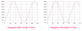

SNR performance decreases at higher frequencies because the effects of jitter get worse.


Types of ADC
There are different type of ADC schemes, each of them has own advantages and disadvantages.

For example, a Flash ADC has drifts and uncertainties associated with the comparator levels, which lead to poor uniformity in channel width and therefore poor linearity.

Poor linearity is also apparent for SAR ADCs, however it is less than that of flash ADCs. Non-linearity in SAR ADC arises from accumulating errors from the subtraction processes.

Wilkinson ADCs can be characterised as most linear ones; particularly, Wilkinson ADCs have the best (smallest) differential non-linearity.


Flash (parallel encoder) ADC
Flash ADCs are made by cascading high-speed comparators. For an N-bit ADC, the circuit employs 2N-1 comparators. A resistive-divider with 2N resistors provides the reference voltage. The reference voltage for each comparator is one least significant bit (LSB) greater than the reference voltage for the comparator. Each comparator produces a 1 when its analogue input voltage is higher than the reference voltage applied to it. Otherwise, the comparator output is 0.
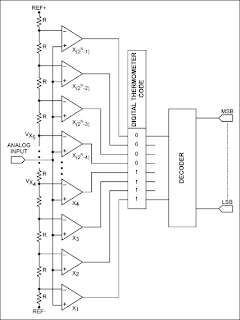
[the Image from the reference, (c) Maxim-ic]

The key advantage of this architecture is very fast conversion times, which is suitable for high-speed low-resolution applications.

The main disadvantage is its high power consumption. The Flash ADC architecture becomes prohibitively expensive for higher resolutions. [the reference used, (c) Maxim-ic]


Successive approximation register ADC

Successive-approximation-register (SAR) ADCs are the majority of the ADC market for medium- and high-resolution. SAR ADCs provide up to 5Msps sampling rates with resolutions from 8 to 18 bits. The SAR architecture allows for high-performance, low-power ADCs to be packaged in small form factors. The basic architecture is shown in Fig.~\ref{fig:SARADC}.
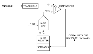
[ the Image from this reference, (c) Maxim-ic]

The analogue input voltage (VIN) is held on a track/hold. To implement the binary search algorithm, the N-bit register is first set to midscale. This forces the DAC output (VDAC) to be VREF/2, where VREF is the reference voltage provided to the ADC.

A comparison is then performed to determine if VIN is less than, or greater than, VDAC. If VIN is greater than VDAC, the comparator output is a logic high, or 1, and the MSB of the N-bit register remains at 1. Conversely, if VIN is less than VDAC, the comparator output is a logic low and the MSB of the register is cleared to logic 0.

The SAR control logic then moves to the next bit down, forces that bit high, and does another comparison. The sequence continues all the way down to the LSB. Once this is done, the conversion is complete and the N-bit digital word is available in the register.

Generally speaking, an N-bit SAR ADC will require N comparison periods and will not be ready for the next conversion until the current one is complete. This explains why these ADCs are power- and space-efficient. Another advantage is that power dissipation scales with the sample rate.[the reference used, (c) Maxim-ic]
Monday, April 11, 2011

Avalanche Photodiodes in Astronomical Adaptive Optics

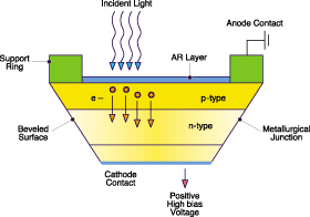
An avalanche photodiode (APD) is a photodiode that internally amplifies the photo-current by an avalanche process. In an APD incoming photons produce electron-hole pairs; however, the APD is operated with a large reverse bias (up to 2 kV), which accelerates the photon-generated electrons. The electrons collide with the atomic lattice, releasing additional electrons via secondary ionisation. These secondary electrons also are accelerated, which results in an avalanche of carriers.

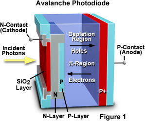
Photons entering the diode first pass through the silicon dioxide layer and then through the n and p layers before entering the depletion region where they excite free electrons and holes, which then migrate to the cathode and anode, respectively. When a semiconductor diode has a reverse voltage bias applied and the crystal junction between the p and n layers is illuminated, then a current will flow in proportion to the number of photons incident upon the junction.


As these electrons collide with other electrons in the semiconductor material, they cause a fraction of them to become part of the photo-current - this process is called avalanche multiplication.

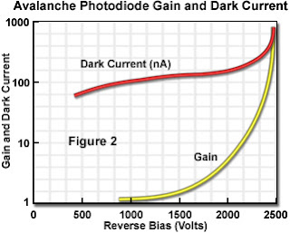
The gain of the APD is changed by the reverse-bias voltage applied (larger bias voltage - larger gain). However, a larger reverse-bias voltage also results in increased noise levels. Excess noise resulting from the avalanche multiplication process places a limit on the useful gain of the APD. The avalanche process introduces excess noise because every photogenerated carrier does not undergo the same multiplication. Avalanche photodiodes are capable of modest gain (500-1000), but exhibit substantial dark current, which increases markedly as the bias voltage is increased.

Overall, avalanche photodiodes are compact and immune to magnetic fields, require low currents, are difficult to overload, and have a high quantum efficiency that can reach 90 percent.


Avalance Photodiodes in Wavefront Sensors
It was reported\cite{takami2004performance} that avalanche photodiodes are used in wavefront sensors for adaptive optics.


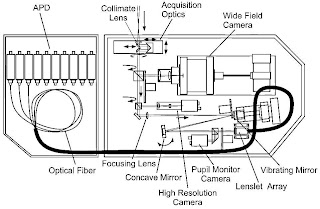
The modulated light intensity signal is sampled at each sub-aperture of a microlens array and fed through optical fibers to photon-counting avalanche photodiode (APD) modules. The current Subaru AO system has 36 sub-apertures.

A benefit of this type of sensor is that one can use photon-counting avalanche photodiodes without readout noise\cite{takami2004performance}, while for Shack-Hartmann
sensors the readout noise of CCD detector becomes the dominant error source for faint guide stars\cite{takami2004performance}. A 1000x1000 cooled CCD (EEV CCD47-20) camera covering a 20 field is used to monitor the guide star.

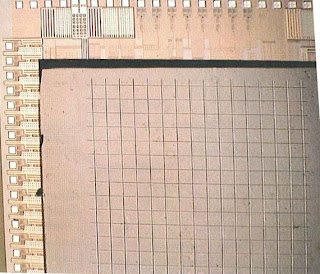
Another proposal\cite{aull2010adaptive} is from Lincoln Laboratory where has been investigating Geiger mode avalanche photodiode arrays integrated with CMOS readout circuits. This type of sensor counts photons digitally within the pixel, enabling data to be read out at high rates without the penalty of readout noise.


It has been demonstrated\cite{aull2010adaptive} a high-fill-factor, 16x16 quad cell APD array with monotonic centroiding response. Devices with a 32x32 format are in fabrication.

However, the dark count rate of the high-fill-factor devices is high compared with other detector technologies, and the mechanisms for this have been investigated. The dark count rate is hypothesised to arise from a combination of tunnelling current at the junction periphery, unsuppressed thermal dark current, and optical self re-triggering\cite{aull2010adaptive}.


Advances in APD for AO
Development of novel circuitry for solid state photon counting devices, based on avalanche photodiodes (PC-APD), was also reported\cite{bonaccini1994novel}. The recent development has improved silicon APDs considerably, reducing the afterpulsing effects, improving the effective Q.E., and reducing the dark current to negligible values. These new APD allow to conceive new quenching circuitry and new applications of solid state photon counters for improved adaptive optics performance\cite{bonaccini1994novel}.

The development of APDs is focusing on high bandwidth, low excess noise, and high gain bandwidth\cite{campbell2004recent}. It has been shown that lower noise and higher gain bandwidth products can be achieved by submicron scaling of the multiplication region thickness and replacing InP in the multiplication layer with Al In As\cite{campbell2004recent}. However, spatial uniformity of the photoresponse at very high gains remains work in progress.


References
\begin{thebibliography}{1}

\bibitem{takami2004performance}
H.~Takami, N.~Takato, Y.~Hayano, M.~Iye, S.~Oya, Y.~Kamata, T.~Kanzawa,
Y.~Minowa, M.~Otsubo, K.~Nakashima, et~al.
\newblock {Performance of Subaru Cassegrain adaptive optics system}.
\newblock {\em PUBLICATIONS-ASTRONOMICAL SOCIETY OF JAPAN}, 56(1):225--234,
2004.

\bibitem{aull2010adaptive}
B.F. Aull.
\newblock {Adaptive optics wavefront sensors based on photon-counting detector
arrays}.
\newblock 2010.

\bibitem{bonaccini1994novel}
D.~Bonaccini, S.D. Cova, M.~Ghioni, R.~Gheser, S.~Esposito, and
G.~Brusa-Zappellini.
\newblock {Novel avalanche photodiode for adaptive optics}.
\newblock 2201:650, 1994.

\bibitem{campbell2004recent}
J.C. Campbell, S.~Demiguel, F.~Ma, A.~Beck, X.~Guo, S.~Wang, X.~Zheng, X.~Li,
J.D. Beck, M.A. Kinch, et~al.
\newblock {Recent advances in avalanche photodiodes}.
\newblock {\em Selected Topics in Quantum Electronics, IEEE Journal of},
10(4):777--787, 2004.

\end{thebibliography}

Saturday, April 2, 2011

Modified Hudgin geometry for Wavefront reconstruction using Fast Fourier Transform

One of the attractive abilities of the FFT WFR is that the filtering construct provides flexibility: reconstruction is accomplished by filtering in the frequency domain and one can modify this filter with negligible computational overhead. It is easy to incorporate filtering options into the
reconstruction filters like noise reduction, modal removal, misalignment, or DM geometry compensation.

Misalignment of the WFS data and the DM geometry.


For example, the misalignment can be compensated: the WFS grid and the DM actuators may be misaligned by shifts along x or y dimensions. If the amount is known, shift slope estimate by a fraction of an actuator spacing such as $(exp[-i 2\pi (\Delta_x k + \Delta_y l)/ N])\Phi$.


Modified Hudgin geometry
For Shack-Hartmann, best the reconstructor is modified Hudgin, for which the
slopes are: $s_x[m,n] = \phi[m+1n,n+0.5] - \phi[m,n+0.5]$.
The reconstruction of the wavefront is performed with the following procedure:
$\begin{matrix} \hat{\Phi}[k,l] & = & \left\{ \begin{matrix} 0 & \mbox{if } k,l = 0 \\ S_x[k,l]\cdot H_x[k,l] + S_y[k,l]\cdot H_y[k,l] & \mbox{otherwise } \end{matrix} \right.\end{matrix}$

The the spatial filters are different: we ahve to shift each slope signal half a
sample along the orthogonal direction:
$ H_x[k,l] = \frac{ (\exp\left[ - \frac{2\pi i \cdot k }{N} \right] -1) \exp(-i\pi
l / N) }{ 4\left( \sin^2\frac{\pi k}{N} + \sin^2\frac{\pi l}{N} \right)} \\ H_y[k,l] = \frac{ (\exp\left[ - \frac{2\pi i \cdot l }{N} \right] -1) \exp(-i\pi
k / N) }{ 4\left( \sin^2\frac{\pi k}{N} + \sin^2\frac{\pi l}{N} \right)} $

Taking the inverse transform $\mathcal{F}^{-1}\hat{\Phi}[k,l] $ produces the
estimate of the wavefront $\hat{\phi}[m, n]$. Such a geometry estimations (see Fig.~\ref{fig:ao2004_3670_modified_Hudgin}) are of
high quality, and it does not suffer from global or local waffle like Fried
geometry.

Modified Hudgin geometry.


That was validated\cite{poyneer2003experimental} in on-sky testing at
Palomar Observatory. In the experiments, the authors of
\cite{poyneer2003experimental} tried out several options for geometries and
filtering, and the modified Hudgin performed best. It is noteworthy that the
regular Hudgin geometry suffered from misalignment-like errors. Finally, the
Fried geometry had excessive local waffle.

Moreover, the modified Hudgin takes half as much computation as the Fried geometry model.

Limitations and Disadvantages of the FTR


Disadvantages
First, if the aperture size in sub-apertures is not a power-of-2, that can cause
performance problems: extensive padding to get to a power-of-2 leads to
increased noise. The FTR requires the square or the pseudo-hex DM geometry. The
non-integer ratio of sub-apertures size or actuator spacing
requires correct re-sampling of estimate.

Advantages
The FTR is fast enough for the ExAO systems and large simulation codes. It provides adaptability with filtering - one can compensate the misalignment and
other errors. The modified Hudgin method does not suffer significantly from the global or local waffle.


The problems in implementation of modified Hudgin
The modified Hudgin still requires the suppression of the piston mode:
if ((rownum == 0)&(colnum == 0))
wavefront(rownum+1, colnum+1) = 0;
else

The original formula for the spatial filters works queer. The additional shift must be like this: $\exp(-i2\pi l / N)$ instead of simply $\exp(-i\pi l / N)$.

Moreover, the code for the different shifts gives slightly different results. The results with the spatial filter:

$$H_x[k,l] = \frac{ (\exp\left[ - \frac{2\pi i \cdot k }{N} \right] -1) \exp(-i2\pi l / N) }{ 4\left( \sin^2\frac{\pi k}{N} + \sin^2\frac{\pi l}{N} \right)} $$

and implemented as a MATLAB code:

H_row = (exp(-(i*2*rownum*pi)/N_row) -1)*(exp(-(i*2*colnum*pi)/N_row)); %% spatial filters for X axis that include the complex conjugate of exponentials
H_column = (exp(-(i*2*colnum*pi)/N_col) -1)*(exp(-(i*2*rownum*pi)/N_col)); %% spatial filters for Y axis that include the complex conjugate of exponentials


gives the reconstruction, shown in Fig.~\ref{fig:wfr_modified_Hudgin_row-col}a. Contrary, the spatial filter of:

$$H_x[k,l] = \frac{ (\exp\left[ - \frac{2\pi i \cdot l }{N} \right] -1) \exp(-i2\pi
k / N) }{ 4\left( \sin^2\frac{\pi k}{N} + \sin^2\frac{\pi l}{N} \right)} $$

with code:

H_row = (exp(-(i*2*rownum*pi)/N_row) -1)*(exp(-(i*2*colnum*pi)/N_row)); %% spatial filters for X axis that include the complex conjugate of exponentials
H_column = (exp(-(i*2*colnum*pi)/N_col) -1)*(exp(-(i*2*rownum*pi)/N_col)); %% spatial filters for Y axis that include the complex conjugate of exponentials

gives better result in the reconstruction, as seen in Fig.~\ref{fig:wfr_modified_Hudgin_row-col}b.

The results of reconstruction for the modified Hudgin algorithm for the row spatial filter: a) row-column relationships with shifts, and b) column-row relationships.


The results of the modified Hudgin geometry are indeed better compared with the standard Hudgin geometry (see the reconstruction with conventional Hudgin FFT WFR (below)

The results of reconstruction with conventional FFT Hudgin.

Monday, March 14, 2011

Adding a probability distribution to another: superimpose the probability distribution

We all learned some probability theory at Uni, but the learning pure theory is one thing, and application of it is slightly different. There is learning, understanding and there is an acceptance, as O'Brien from 1984 has told. The topic of this post is how to superimpose two (or more) distributions.

Introduction
For instance, we have a skewed probability density function and the data generated according to it. Let it be Log-Normal distribution:

$p_{LogNorm}(x;\mu, \sigma) = \frac{1}{x\sqrt{2\pi\sigma^2}}\, e^{-\frac{\left(\ln x-\mu\right)^2}{2\sigma^2}}$

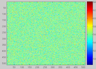
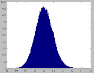
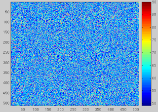
with parameters $\mu = 4.0246$ and $\sigma = 0.0350$ respectively. The data looks like:
OK, so far so good: the data is noisy and have values from about 50 to about 64, that is in consistency with the probability probability density function:

The pdf was numerically estimated using hist function in MATLAB.

The Problem:
I need to make a new pdf that is superimposed by the uniform distribution. The idea is to make a distribution with very long "tail". Well, we can do it accurately, using theoretical expressions of sum of random variables (see, for instance, Probability and random processes by Stark and Woods, Chapter 3). But after all, we need to generate the data using it and not just tinker with it.


The solution
Let's say, we need to add some uniform distribution in order to make the "tail" of summary distribution longer. OK, we can easily generate uniform distribution using rand function in MATLAB or Octave. Generate a uniform distribution of random numbers on a specified interval [a,b]. To do this, multiply the output of rand by (b-a) then add a. Here is MATLAB code:
Isize = 256;
a=5;
b=50;
I = a + (b-a)*rand(Isize);
Now it is not obvious: if we just add two distributions (either in spatial domain or in Fourier domain using point-wise addition), we will get wrong result:

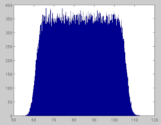
What has happenned? Well, because this is uniform distribution, it just wiped out our gentle Log-Normal data. Hence we need to attenuate the amount of the uniform distribution that we add.

One solution is to add, say, every second data point. Nice idea, but not clever: our data will be periodic that is not desirable. The better solution is to generate another uniform distribuiton [0,1] and make it like a mask for addition of desired data points.

In order to attenuate the influence of the other distribution, we need to add only a few point from the other distribution. Here is the example:

z = ones(Isize); %% creating a mask of the adding new pdf.
addition_percentage = 0.6;
z = rand(Isize,Isize);
z(z>addition_percentage) = 0;

%%% Erasing the unnecessary points from the other distribution
I = I.*z;
Here our mask will be like:

0 0 0.1157 0.2088 0.5074

0.3981 0 0.3826 0.3936 0.1435

0 0.0476 0.5989 0.5155 0.5239

0 0 0 0.4117 0

0 0 0.0858 0 0

0 0.4345 0.4846 0.4592 0

0 0.4591 0.3690 0.1043 0

We can use ceil(z) to make it just 0 or 1, but in our case we want the "tail" to decay. Multiplication of two uniform distribution is not a longer uniform distribution, as one might think :-) It will be triangular-shaped and, if we continue to multiply it more, will tend to be Gaussian, as followed by CLT:
The Central Limit Theorem (CLT) states conditions under which the mean of a sufficiently large number of independent and identically distributed random variables, each with finite mean and variance, will be approximately normally distributed.
So then we just add:
I2 = I+Ilong;
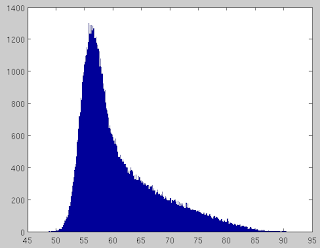
where I is uniform distribution multiplied by uniform mask (now will be triangular-like), and Ilong is long-tailed distribution. The result pleases the eye, the mind and the soul:
That's exactly what we desired, and the data is appropriate:
Now it's a good time to write a huge article to SIAM Journal entitled "Recent ground-breaking advances in Advanced Probability Theory" :-)


Various thoughts and jots

The sum of two normal distributions is itself a normal distribution:

N(mean1, variance1) + N(mean2, variance2) ~ N(mean1 + mean2, variance1 + variance2)

This is all on wikipedia page.

Be careful that these really are variances and not standard deviations.

Monday, March 7, 2011

Bilaterial filter for Photon noise suppression

For the controller in adaptive optics system, the photon shot noise can be a serious issue. But there is a promising results\cite{bilaterialshotnoise} in shot noise filtering using Bilaterial filter. Bilateral filtering was proposed in\cite{tomasibilateral} as a non-iterative method for edge-preserving smoothing.

The MATLAB implementation of bilateral filter can be found here or here.

The bilateral filter is a local filter\cite{aurich1995non,smith1997susan,tomasibilateral} that reduces noise in images while preserving edges by means of non-linear combination of local pixel values. However the problem is to find optimal parameter for the bilateral filter in each case of the signal level.

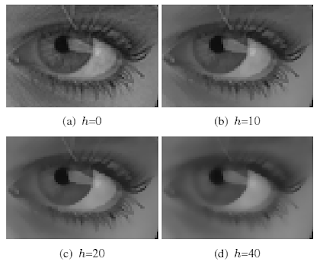
Bilateral filtering using a $5\times5$ square window as $\beta$ and a variable $h$


The bilateral filter replaces a pixel value in an image by a weighted mean of its neighbours considering both their geometric closeness and photometric similarities\cite{bilaterialshotnoise}.

The Gaussian bilateral filter version has a set of parameters that have an important impact on filtering behaviour and performance. The Gaussian bilateral filter is the most used on practice\cite{paris2009fast}:

$v(x) = \frac{1}{C(x)} \sum_{\beta} exp(-\frac{|x-y|^2}{\rho^2}) exp(-\frac{|u(y) - u(x)|^2}{h^2})$

where $\beta$ represents the sliding window, y is a set of 2-D pixel
positions in the sliding window, and x is the 2-D position of
the centred pixel in the sliding window. The u(x) is the intensity
of the pixel at the x position in the original image, v(x) is
the estimated pixel at the x position, $\rho$ and $h$ are the standard deviation of the Gaussian distribution of the geometrical and the intensity weight respectively.

Parameter $\rho$ can be chosen considering the size of the convolution kernel.

Parameter h has to be chosen considering the level of filtering needed for the application.

The paper\cite{bilaterialshotnoise} presents the approach of adaptive parameters choice. But it is more interesting to see the actual noise suppression capabilities of the bilateral filter.


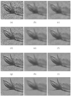
From left to right, the first column shows the noisy images, the second column shows the bilateral filtered images with a h parameter fixed to 100, the third column shows the results obtained with our proposed method.


As stated earlier, the bilateral filter smoothing properties
vary with h. Intuitively we can assume that a low h should be preferable in low noise level, whereas a high h may be necessary in high-noise conditions.


REFERENCES:

\bibitem{bilaterialshotnoise}
H.~Phelippeau, H.~Talbot, M.~Akil, and S.~Bara.
\newblock {Shot noise adaptive bilateral filter}.
\newblock pages 864--867, 2008.

\bibitem{tomasibilateral}
C.~Tomasi and R.~Manduchi.
\newblock {Bilateral filtering for gray and color images}.
\newblock pages 839--846, 1998.

\bibitem{aurich1995non}
V.~Aurich and J.~Weule.
\newblock {Non-linear gaussian filters performing edge preserving diffusion}.
\newblock pages 538--545, 1995.

\bibitem{smith1997susan}
S.M. Smith and J.M. Brady.
\newblock {SUSAN - A new approach to low level image processing}.
\newblock {\em International journal of computer vision}, 23(1):45--78, 1997.

\bibitem{paris2009fast}
S.~Paris and F.~Durand.
\newblock {A fast approximation of the bilateral filter using a signal
processing approach}.
\newblock {\em International journal of computer vision}, 81(1):24--52, 2009.

Wednesday, March 2, 2011

A little note on Shack-Hartmann wavefront sensor

A well-known Hartmann test\cite{hartmann1900} devised initially for telescope optics control was adapted for adaptive optics. The design of this sensor was based on an aperture array that had been developed by Johannes Franz Hartmann\cite{platt2001history} as a means to trace individual rays of light through the optical system of a large telescope, thereby testing the quality of the image\cite{hartmann1900}. In the late 1960s Shack and Platt\cite{shackhartmproduction} modified a Hartmann screen by replacing the apertures in an opaque screen with an array of lenslets.


It is interesting that the construction of SH WFS is simple yet effective; in fact, first lenslet arrays were kithcen-made\cite{platt2001history}:
Platt made a mount for compression, moulding a 1-mm-thick square plate of optical grade thermal plastic (Plexiglass) between the two Cervet squares. [...] Each heating and cooling cycle in the moulding process took several hours. So, Platt decided to work all day and most of the night in his wife's kitchen. His wife's electric knife sharpener was used to trim the Plexiglass plates. Her apron and oven mittens were also used to remove the moulds from the oven. After a few weeks, the process was perfected and good quality lens arrays were being produced. For at least the next 5 years, all lens arrays used in Shack-Hartmann wavefront sensors were made by Platt in his wife's kitchen.
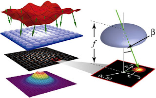
The principle of the Shack-Hartmann (SH) wavefront sensor (WFS) is the following. An image of the exit pupil is projected onto a lenslet array. Each lens takes a small part of the aperture (sub-aperture), and forms an image of the source. When an incoming wavefront is planar, all images are located in a regular grid defined by the lenslet array geometry. As soon as the wavefront is distorted, images become displaced from their nominal positions. Displacements of image centroids in two orthogonal directions $x,y$ are proportional to the average wavefront slopes in $x,y$ over the sub-apertures.


Centroiding
For a sampled light intensity $I_{i,j}$, positions of spots $x_{c_k}$ and $y_{c_k}$ are:

$$ x_{c_k} = \frac{\sum_{i,j} x_{i,j}I_{i,j}}{\sum_{i,j} I_{i,j}},\,\,\,\,
y_{c_k} = \frac{\sum_{i,j} y_{i,j}I_{i,j}}{\sum_{i,j} I_{i,j}},
$$

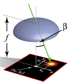
Resulting local direction angle $\beta$:
$$
\beta_x \approx (x_{c_k} - x_{r_k})\frac{L_x}{f},\,\,\,\,
\beta_y \approx (y_{c_k} - y_{r_k})\frac{L_y}{f},
$$

where $L_x$ is a size of the photosensor's pixel and $f$ is the focus length of the lenslet.


\vspace{3ex}\textit{Advantages}: predictable results, simple and effective construction, ability to simultaneously determine $x$ and $y$ slopes.

\vspace{3ex}\textit{Disadvantages}: centroiding algorithm is computationally-intensive.

\vspace{3ex}Shack-Hartmann wavefront sensor is the most popular: its precision and accuracy can be scaled over a huge range through the choice of lenslet array and detector.


Typical WFS SH characteristics

Typical parameters for the Shack-Hartmann sensor in the year 2010 are:
  • Aperture Size 5.95 mm x 4.76 mm. Max.
  • Camera Resolution 1280 x 1024 Pixels Max.
  • Pixel Size $4\dots5.5 \mu$m
  • lenslet size 300$\mu m$
  • lenslet focus distance 7 mm
  • Number of Subapertures $\leq 150$


References \begin{thebibliography}{1}

\bibitem{hartmann1900}
J.~Hartmann.
\newblock {Bemerkungen {\"u}ber den Bau und die Justirung von Spektrographen}.
\newblock {\em Z. Instrumentenkd}, 20:47, 1900.

\bibitem{platt2001history}
B.C. Platt.
\newblock {History and principles of Shack-Hartmann wavefront sensing}.
\newblock {\em Journal of Refractive Surgery}, 17(5):573--577, 2001.

\bibitem{shackhartmproduction}
R.V. Shack and B.C. Platt.
\newblock {Production and use of a lenticular Hartmann screen}.
\newblock {\em J. Opt. Soc. Am}, 61(5):656, 1971.

\end{thebibliography}

Monday, February 21, 2011

When the Poisson distribution can be approximated as Gaussian?

In many articles that deal with noise, and especially in photosensors, there is a usual mantra assume the noise as a Gaussian distributed. Such mantra is said even to processes that are Poissonian by the very nature (photon shot noise). The question: ``how many arrivals can justify the Gaussian approximation?'' is usually answered in vague term ``many''. Well, how many!?

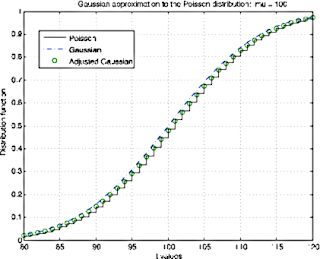
Good question. Some authors say\cite{mendenhallstatistics} that more then 1000 arrival events can be considered as Gaussian. And it seems to be reasonable, as shown [the picture from here]:

The approximation of Poisson distribution by Gaussian is performed usually to simplify the calculations. However, the approximation is not simple. In\cite{poisson2gaussapprox} was shown that the usual approximation of a Poisson density function with mean $m$ by a Gaussian density function with mean $\mu$ and variance $\sigma$ both equal to $m$ is in general not satisfactory for error-rate calculations. A short letter to IEEE Transactions describes a modified Gaussian approximation to a Poisson distribution which, unlike the usual Gaussian approximation, gives good agreement on the tails of the distribution.


We can express Poisson distribution $p(n, m)$ in terms of Gaussian $g(n,m)$ as follows\cite{poisson2gaussapprox}:

$$p(n,m) = \left(\frac{1}{\sqrt{2\pi m}}\right)^{\frac{1}{1+\alpha}} \exp\left[ -\frac{\beta}{1+\alpha} - \frac{(n-m)^2}{2m(1+\alpha)} \right] $$


Thus a Gaussian that better approximates Poisson $p(n, m)$ on the tails has the same mean as $p(n, m)$ but has variance $m(1 + \alpha)$.


The parameters $\alpha$ and $\beta$ can be expressed via $\mu$ as:


$\alpha = (0.080\mu^2 - 0.230\mu + 1.260)^{-2}$


and


$\beta = (0.0667\mu^2 -0.3933\mu + 0.810)^{-1}$


References:

\begin{thebibliography}{1}

\bibitem{mendenhallstatistics}
W.~Mendenhall and T.~Sincich.
\newblock {Statistics for Engineering and the Sciences}.
\newblock 2006.

\bibitem{poisson2gaussapprox}
W.M. Hubbard.
\newblock The approximation of a poisson distribution by a gaussian
distribution.
\newblock {\em Proceedings of the IEEE}, 58(9):1374 -- 1375, 1970.

\end{thebibliography}

Related Posts Plugin for WordPress, Blogger...