Monday, December 1, 2008

Correlators architecture: a small survey

The most common types of correlators are surveyed in this post. The aim is to provide some basic concepts about correlators such as 4-f correlator (Vander Lugt correlators), Joint-transform correlator, and some others. Only 2-D correlators are surveyed.


Vander Lugt (4-f) Correlator

Such type of correlator is mainly the spatial frequency filter. To obtain the cross-correlation of g(x,y) and h(x,y) , we need to synthesize a consistent to h(x,y) filter H(u,v) .

Figure 1: 4-f correlator's scheme
PE coding scheme

Thus, multiplication of Fourier filters occurs in Vander Lught's correlators. And you need to record a hologram or interfering image of the reference image. It is pretty difficult if you want to operatively compare images. After synthesizing of corresponding correlation filter, one should set it up in the P2 plane and turn it by 180 degrees.

The intensity of correlation peaks are connected with similarity of reference image and input scene. Colier (page 557): there is a difficulty. Because of linearity of our correlator and presence of loads of correlation signals.

It is interesting to note that correlation peak wouldn't be the only one, and it's width would be different.

Joint transform correlator

Colier page 563 writes about it: JTC correlator has many practical applications. To do it best, one should use spatial light modulators.

In the JTC correlators, it is much less strict rules for positioning the reference image. It is best for real-time applications, when both input scene and reference image are shine upon the correlator.

Figure 2: JTC scheme

However, the presence of complex or expensive elements complicates the creation of simple and low-priced devices of this type.

Saturday, November 1, 2008

High dynamic range imagery

The dynamic range (DR) of modern solid-state photo sensors is generally not wide enough to image natural and some artificial scenes. This is especially the case for CMOS image sensors, since their read noise and DSNU are typically larger than CCDs. For reference, standard CMOS image sensors have a DR of 40-60 dB, CCDs around 60-70 dB; special CMOS imagers that employ continuous-time logarithmic readout achieve DR up to 140 dB, but they suffer from the loss of contrast and an increase of noise [1,2,3]. In contrast, the human vision system exhibits an enormous optical dynamic range of about 200 dB from the scotopic threshold to the glare limit [4]. Such capability is also required in many imaging applications.


To overcome DR limitations of photo sensors, several approaches were presented. Such approaches can be divided to hardware approaches (creating new architectures of sensors), software approaches (using colour light filters or multi-exposure of the same CMOS/CCD sensors), and hybrid hardware-software approaches (using spatial modulators, combining sensors with new architecture and multi-exposure technologies).

Hardware methods of HDR vision

Besides Active Pixel Sensor [5,6], many new sensor's architectures were presented recently. For example, a CMOS imager [2] that automatically selects a single optimum integration time and readout gain out of a variety of available integration times and gains individually for each pixel. Some CMOS approaches published in the open literature that rely on discrete-time integration either employ multiple sampling [7], sometimes combined with non-linear analogue-to-digital (A/D) conversion [8], or use non-linear integration [9]. An interesting approach is to design CMOS imagers with purely local on-chip brightness adoption [10].

Another way of hardware HDR imaging is to use ``smart sensors'' approach. ``Smart sensors'' have augmented photo-sensors with local processing for tasks such as edge detection, motion sensing and tracking. Mead's silicon retina and adaptive retina [11] chips were among the first to mimic vertebrate retina computations, and inspired many later efforts [12]. For example, in Mitsubishi's artificial retina [13] each photodetector's sensitivity was controllably modulated by others nearby to avoid saturation and aid in fast edge detection. In [14], a novel solid state image sensor is described where each pixel on the device includes a computational element that measures the time it takes to attain full potential well capacity.

It is also worth noting the approach to HDR imaging that uses a custom detector [15,16] where each detector cell includes two sensing elements (potential wells) of different sizes (and hence sensitivities). A general purpose logarithmic camera suitable for applications from family photographs to robotic vision to tracking and surveillance is presented [17].

Thus it can be concluded that hardware HDR solutions are compact and integrated (there is no need to use powerful computers for image processing), and ability to receive very wide dynamic range of images. The only disadvantage is the price of such photosensors: many of them are state-of-the-art devices and it is sometimes difficult to provide HDR-sensors with large amount of elements (5 Mpix and more).

Software methods of HDR vision

Many high dynamic range (HDR) photography methods were proposed that merge multiple images with different exposure settings [18,19,20]. Nayar et al. [21] has proposed a suite of HDR techniques that included spatially-varying exposures and adaptive pixel attenuation, and micro-mirror arrays to re-aim and modulate incident light on each pixel sensor [22]. Numerous reconstruction and tone mapping methods [23,20,18] were proposed for digital HDR photography. At each exposure setting, a different range of intensities can be measured reliably. Fusing the data from all the exposures [20,18] results in a single high dynamic range (HDR) image.

It is worth noting a simple and efficient method of obtaining HDR images from conventional photo sensor using Bayer colour filters array - Spatially Varying Pixel Exposures [24,25]. The idea is to assign different (fixed) exposures to neighbouring pixels on the image detector. When a pixel is saturated in the acquired image it is likely to have a neighbour that is not, and when a pixel produces zero brightness it is likely to have a neighbour that produces non-zero brightness.

Hence software methods are tend to be less expensive because it is possible to use conventional photosensors. For HDR images obtaining it is necessary only to develop special software; the disadvantages of such approaches are lower DR images and necessity to use external computers for image processing. But for portable machine vision systems software HDR methods can be the only one possibility.

Hybrid hard'n'soft HDR approaches

Most of hybrid hard'n'soft HDR methods use the combination of conventional CMOS or CCD photo sensor and light modulators (either LCD or light filters). For example, Adaptive Dynamic Range (ADR) concept was introduced in [21,26] were LCD ligth modulators as spatial filters were used. Such ADR concept is suitable not only for stil images, but for video sequences, too.

Simplest approach is to use multiple image detectors: beam splitters [27] are used to generate multiple copies of the optical image of the scene. Each copy is measured by an image detector whose exposure is preset by using an optical attenuator or by adjusting the exposure time of the detector.

Another approach is mosaicking with Spatially Varying Filter. Recently, the concept of generalized mosaicking [28,29], was introduced where a spatially varying neutral density filter is rigidly attached to the camera. When this imaging system is rotated, each scene point is observed under different exposures.

Hybrid methods of HDR imaging are tend to use software HDR methods, conventional photosensors, and external optical devices to control input scene's lightness. Advantages of hybrid methods are inexpensiveness and ability to receive wider DR images than pure software methods. But machine vision devices that use hybrid HDR approach are more cumbersome and hence may not be suitable for compact applications such as in-vehicle systems.

Bibliography


1
J. Huppertz, R. Hauschild, B. J. Hosticka, T. Kneip, S. Mller, and M.Schwarz.
Fast CMOS imaging with high dynamic range.
In Proc. Workshop Charge Coupled Devices & Advanced Image Sensors, Bruges, Belgium, pp. R7-1-R7-4., June 1997.
2
Michael Schanz, Christian Nitta, Arndt Bumann, Bedrich J. Hosticka, and Reiner K. Wertheimer.
A high-dynamic-range CMOS image sensor for automotive applications.
IEEE Journal of Solid-State Circuits, Vol. 35, No. 7:932-938, July 2000.
3
M. Schanz, W. Brockherde, R. Hauschild, B. J. Hosticka, and M.Schwarz.
Smart CMOS image sensor arrays.
IEEE Trans. Electron Devices, 44:1699-1705, Oct. 1997.
4
T. N. Cornsweet.
Visual Reception.
New York, NY: Academic, 1970.
5
O. Yadid-Pecht and A. Belenky.
In-pixel autoexposure CMOS APS.
IEEE Journal of Solid-State Circuits, vol. 38, no. 8:1425-1428, August 2003.
6
Orly Yadid-Pecht.
Active pixel sensor (aps) design - from pixels to systems.
Lectures.
7
O. Yadid-Pecht and E. Fossum.
Wide intrascene dynamic range CMOS APS using digital sampling.
IEEE Trans. Electron Devices, 44:1721-1723, Oct. 1997.
8
B. Fowler D. Yang, A. El Gamal and H. Tian.
A $ 640\times 512$ CMOS image sensor with ultrawide dynamic range floating-point pixel-level adc.
IEEE J. Solid-State Circuits, 34:1821-1834, Dec. 1999.
9
K. Brehmer S. J. Decker, R. D. McGrath and C. G. Sodini.
A $ 256 \times 256$ cmos imaging array with wide dynamic range pixels and column-parallel digital output.
IEEE J. Solid-State Circuits, 33:2081-2091, Dec. 1998.
10
R. Hauschild, M. Hillebrand, B. J. Hosticka, J. Huppertz, T. Kneip, and M. Schwarz.
A cmos image sensor with local brighness adaption and high intrascene dynamic range.
In Proc. Eur. Solid-State Circuit Conf. (ESSCIRC'98), The Hague, the Netherlands, pp. 308-311, Sept. 22-24, 1998.
11
C. Mead.
Analog VLSI implementation of neural systems, chapter Adaptive Retina, pages 239-246.
Kluwer, 1989.
12
A. Moini.
Vision chips or seeing silicon, 1997.
13
E. Funatsu et al.
An artificial retina chip with a 256x256 array of n-mos variable sensitivity photodetector cells.
Proc. SPIE. Machine Vision App., Arch., and Sys. Int. IV, 2597:283-291, 1995.
14
V. Brajovic and T. Kanade.
A sorting image sensor: An example of massively parallel intensity-to-time processing for low-latency computational sensors.
In Proc. of IEEE Conference on Robotics and Automation, pages 1638-1643, April 1996.
15
R. J. Handy.
High dynamic range ccd detector/imager.
Technical report, U.S. Patent 4623928, November 1986.
16
M. Inuiya M. Konishi, M. Tsugita and K. Masukane.
Video camera, imaging method using video camera, method of operating video camera, image processing apparatus and method, and solid-state electronic imaging device.
Technical report, U.S. Patent 5420635, May 1995.
17
J. Tumblin, A. Agrawal, and R. Raskar.
Why i want a gradient camera.
In Proc. of IEEE CVPR, 2005.
18
S. Mann and R. Picard.
Being ``undigital'' with digital cameras: Extending dynamic range by combining differently exposed pictures.
In Proc. IST`s 48th Annual Conf., pages 422-428, 1995.
19
S. Winder S. B. Kang, M. Uyttendaele and R. Szeliski.
High dynamic range video.
ACM Trans. on Graphics, 22(3):319-325, July 2003.
20
P. E. Debevec and J. Malik.
Recovering high dynamic range radiance maps from photographs.
SIGGRAPH , 1997.
21
S.K. Nayar and V. Branzoi.
Adaptive dynamic range imaging: Optical control of pixel exposures over space and time.
IEEE International Conference on Computer Vision, Vol.2:1168-1175, Oct, 2003.
22
V. Branzoi S. K. Nayar and T. Boult.
Programmable imaging using a digital micromirror array.
CVPR., 1:436-443, 2004.
23
M.D. Grossberg and S.K. Nayar.
Determining the camera response from images: What is knowable?
IEEE Trans. Pattern Analysis and Machine Intelligence, vol. 25, No 11:1455-1467, 2003.
24
S. K. Nayar and T. Mitsunaga.
High dynamic range imaging: Spatially varying pixel exposures.
IEEE Conference on Computer Vision and Pattern Recognition (CVPR), Vol. 1:pp.472-479, June, 2000.
25
Srinivasa G. Narasimhan and Shree K. Nayar.
Enhancing resolution along multiple imaging dimensions using assorted pixels.
IEEE Transactions on Pattern Analysis and Machine Intelligence, vol. 27, No. 4:pp. 518-530, April 2005.
26
Hidetoshi Mannami, Ryusuke Sagawa, Yasuhiro Mukaigawa, Tomio Echigo, and Yasushi Yagi.
High dynamic range camera using reflective liquid crystal.
In Proc. IEEE International Conference on Computer Vision Rio de Janeiro, October 14-20, 2007.
27
K. Saito.
Electronic image pickup device.
Technical report, Japanese Patent 07-254965, February 1995.
28
Y.Y. Schechner and S.K. Nayar.
Generalized Mosaicing: High Dynamic Range in a Wide Field of View.
International Journal on Computer Vision, 53(3):245-267, Jul 2003.
29
M. Aggarwal and N. Ahuja.
High dynamic range panoramic imaging.
In Proc. of International Conference on Computer Vision (ICCV), 1:2-9, 2001.

Wednesday, October 1, 2008

A scrutiny investigations in PixeLink's CMOS cameras: rolling shutter and all around

Active Pixel Sensors (text from [1])

A sensor with an active amplifier within each pixel was proposed [2]. Figure 1 shows the general architecture of an APS array and the principal pixel structure.

Figure 1: General architecture of an APS array (picture from work [1]).

The pixels used in these sensors can be divided into three types: photodiodes, photogates and pinned photodiodes [1].

Photodiode APS

The photodiode APS was described by Noble [2] and has been under investigation by Andoh [3]. A novel technique for random access and electronic shuttering with this type of pixel was proposed by Yadid-Pecht [4].

The basic photodiode APS employs a photodiode and a readout circuit of three transistors: a photodiode reset transistor (Reset), a row select transistor (RS) and a source-follower transistor (SF). The scheme of this pixel is shown in Figure 2.

Figure 2: Basic photodiode APS pixel (picture from work [1]).

Generally, pixel operation can be divided into two main stages, reset and phototransduction.

(a) The reset stage. During this stage, the photodiode capacitance is charged to a reset voltage by turning on the Reset transistor. This reset voltage is read out to one of sample-and-hold (S/H) in a correlated double sampling (CDS) circuit [5]. The CDS circuit, usually located at the bottom of each column, subtracts the signal pixel value from the reset value. Its main purpose is to eliminate fixed pattern noise caused by random variations in the threshold voltage of the reset and pixel amplifier transistors, variations in the photodetector geometry and variations in the dark current [1].

(b) The phototransduction stage. During this stage, the photodiode capacitor is discharged through a constant integration time at a rate approximately proportional to the incident illumination. Therefore, a bright pixel produces a low analogue signal voltage and a background pixel gives a high signal voltage. This voltage is read out to the second S/H of the CDS by enabling the row select transistor of the pixel. The CDS outputs the difference between the reset voltage level and the photovoltage level [1].

Because the readout of all pixels cannot be performed in parallel, a rolling readout technique is applied.

Readout from photodiode APS

All the pixels in each row are reset and read out in parallel, but the different rows are processed sequentially. Figure 3 shows the time dependence of the rolling readout principle.

Figure 3: Rolling readout principle of the photodiode APS (picture from work [1]).

A given row is accessed only once during the frame time (Tframe). The actual pixel operation sequence is in three steps: the accumulated signal value of the previous frame is read out, the pixel is reset, and the reset value is read out to the CDS. Thus, the CDS circuit actually subtracts the signal pixel value from the reset value of the next frame. Because CDS is not truly correlated without frame memory, the read noise is limited by the reset noise on the photodiode [1]. After the signals and resets of all pixels in the row are read out to S/H, the outputs of all CDS circuits are sequentially read out using X-addressing circuitry, as shown in Figure 2.

Other types are global shutter and fast-reset shutter, but such things are out of scope of this note.

Rolling shutter

In electronic shuttering, each pixel transfers its collected signal into a light-shielded storage region. Not of all CMOS imagers are capable of true global shuttering. Simpler pixel designs, typically with three transistors (3T), can only offer a rolling shutter [6]. Each row will represent the object at a different point of time, and because the object is moving, it will be at different point in space.

More sophisticated CMOS devices (4T and 5T pixels) can be designed with global shuttering and exposure control (EC) [6].

Typically, the rows of pixels in the image sensor are reset in sequence, starting at the top of the image and proceeding row by row to the bottom. When this reset process has moved some distance down the image, the readout process begins: rows of pixels are read out in sequence, starting at the top of the image and proceeding row by row to the bottom in exactly the same fashion and at the same speed as the reset process [7].

The time delay between a row being reset and a row being read is the integration time. By varying the amount of time between when the reset sweeps past a row and when the readout of the row takes place, the integration time (hence, the exposure) can be controlled. In the rolling shutter, the integration time can be varied from a single line (reset followed by read in the next line) up to a full frame time (reset reaches the bottom of the image before reading starts at the top) or more [7].

With a Rolling Shutter, only a few rows of pixels are exposed at one time. The camera builds a frame by reading out the most exposed row of pixels, starting exposure of the next unexposed row down in the ROI, then repeating the process on the next most exposed row and continuing until the frame is complete. After the bottom row of the ROI starts its exposure, the process ``rolls'' to the top row of the ROI to begin exposure of the next frame's pixels [8].

The row read-out rate is constant, so the longer the exposure setting, the greater the number of rows being exposed at a given time. Rows are added to the exposed area one at a time. The more time that a row spends being integrated, the greater the electrical charge built up in the row's pixels and the brighter the output pixels will be [8]. As each fully exposed row is read out, another row is added to the set of rows being integrated (see Fig. ).

Figure 4: Rolling shutter in work (picture from work [8]).

If there is a requirement of shooting with photoflash, there must be succeed some conditions. The operation of a photoflash with a CMOS imager [7] operating in rolling shutter mode is as follows:

  1. The integration time of the imager is adjusted so that all the pixels are integrating simultaneously for the duration of the photoflash;
  2. The reset process progresses through the image row by row until the entire imager is reset;
  3. The photoflash is fired;
  4. The imager is read out row by row until the entire imager is read out.

The net exposure in this mode will result from integrating both ambient light and the light from the photoflash. As previously mentioned, to obtain the best image quality, the ambient light level should probably be significantly below the minimum light level at which the photoflash can be used, so that the photoflash contributes a significant portion of the exposure illumination. Depending on the speed at which the reset and readout processes can take place, the minimum exposure time to use with photoflash may be sufficiently long to allow image blur due to camera or subject motion during the exposure. To the extent that the exposure light is provided by the short duration photoflash, this blur will be minimized.


Bibliography


1
Orly Yadid-Pecht.
Active pixel sensor (aps) design - from pixels to systems.
Lectures.
2
P. Noble.
Self-scanned image detector arrays.
IEEE Trans. Electron Devices, ED-15:202, 1968.
3
J. Yamazaki M Sagawara Y. Fujita K. Mitani Y. Matuzawa K. Miyata F. Andoh, K. Taketoshi and S. Araki.
A 250,000 pixel image sensor with FET amplification at each pixel for high speed television cameras.
IEEE ISSCC, pages 212-213, 1990.
4
R. Ginosar O. Yadid-Pecht and Y. Diamand.
A random access photodiode array for intelligent image capture.
IEEE J. Solid-State Circuits, SC-26:1116-1122, 1991.
5
J. Hynecek.
Theoretical analysis and optimization of CDS signal processing method for CCD image sensors.
IEEE Trans. Nucl. Sci., vol.39:2497-2507, Nov. 1992.
6
DALSA corp.
Electronic shuttering for high speed cmos machine vision applications.
Technical report, DALSA Corporation, Waterloo, Ontario, Canada, 2005.
7
David Rohr.
Shutter operations for ccd and cmos image sensors.
Technical report, Kodak, IMAGE SENSOR SOLUTIONS, 2002.
8
PixeLink.
Pixelink product documentation.
Technical report, PixeLink, December, 2007.

Monday, August 18, 2008

How To Write A Scientific Article

A technical paper consists of four sections: Introduction, Formulation of the problem, Results, Conclusion, and Acknowledgements. The purpose of each section is as follows.


Section I: Introduction
The introduction should do the following:
1. Open up the subject.
"Information encryption techniques have been an important and active research area from ancient time to nowadays, which involves a number of applications such as...
"

2. Survey past work relevant to this paper.
"Recently, various methods based on information optics for high dimensional data encryption and decryption have been explored to expand the degrees of freedom for key design and, therefore, to increase the security level of the entire information encryption system [1–6]...."

3. Describe the problem addressed in this paper
,
and show how this work relates to, or arguments, previous work.
"In this paper, we present an alternative data encryption technique based on virtual-optics imaging system..."

4. Describe the assumptions made in general terms
,
and state what results have been obtained. This gives the reader an initial overview of what problem is addressed in the paper and what has been achieved.
"We analyse the sensitivities for some of parameters of such a virtual optics imaging system, with which one is able to design..."

5. Overview the contents of the paper.

``Section II contains our formulation of the problem. Section III contains the experimental data...''


Section II: Formulation of the Problem
This section should do three things:
1. Define the problem to be considered in detail.
Typically this section might begin with something like:
"Consider a virtual–optical imaging system (VOIS) with a single lens. It is schematically shown in Fig. 1..."
The discussion should proceed in this way until the problem is completely defined.

2. Define all terminology and notation used.

Usually the terminology and notation are defined along with the problem itself.
"We refer to as the discrete Fresnel diffraction (DFD) transformation and express it as following
equation.."


3. Develop the equations

on which your results will be based and/or describe any experimental systems.
"In addition, the transmission function of imaging lens should also be described with its discrete
mode in order to carry out numerical simulation: <math here> "


Section III: Results
This section presents the detailed results you have obtained.
If the paper is theoretical, you will probably show curves obtained from your equations.
If the paper is experimental, you will be presenting curves showing the measurement results.
In order to choose the proper curves to present, you must first be clear what point you are trying to convey to the reader. The curves can then be chosen to illustrate this point. Whether your paper is theoretical or experimental, you must provide a careful interpretation of what your results mean and why they behave as they do.


Section IV: Conclusion
This section should summarize what has been accomplished in the paper.
Many readers will read only the Introduction and Conclusion of your paper. The Conclusion should be written so they can be understood by someone who has not read the main work of the paper. This is the common format for an engineering paper. Of course, the names of the sections may differ slightly from those above, but the purpose of each section will usually be as described. Some papers include additional sections or differ from the above outline in one way or another. However, the outline just presented is a good starting point for writing a technical paper.


Section V: Acknowledgements
It is good idea to mention here grant programs and people who contributed in the paper. Usually no more than 3-4 sentences.


References:
This post is based on "Fourteen Steps to a Clearly Written Technical Paper" by R. T. Compton, Jr. Examples of text are used from the article: Xiang Peng, Zhiyong Cui, and Tieniu Tan, Information encryption with virtual-optics imaging system, Optics Communications, 2002, 212:235--245.

Thursday, August 14, 2008

Optical encryption attacks to Double Random Phase Encryption

Double Random Phase Encryption (DRPE) technique has been criticised recently for poor security and low cryptography resistance because of its linearity. Recently has the security of DRP started to be thoroughly analysed and a few weaknesses were reported [1,2,3].

Double Random Phase Encryption technique

As it shortly described in [4], the image to be encrypted P is immediately followed by a first random phase mask, which is the first key X. Both the image and the mask are located in the object focal plane of a first lens (see Fig. 1).


In the image focal plane of this lens is therefore obtained the Fourier transform (FT) of the product $ P\cdot X$ . This product is then multiplied by another random phase mask that is the second key Y. Lastly, another FT is performed by a second lens to return to the spatial domain. Since the last FT does not add anything to the security of the system, we will perform all our analyses in the Fourier plane. The ciphered image C is then:

$\displaystyle C = Y \cdot \mathcal{F}(P\cdot X)$ (1)

where F stands for the Fourier transform operation. In most of the paper, we will assume that P is a grey-level image.


Attacks to the DRPE


Several attacks are proposed against the double random phase encryption scheme. Of source, as it mentioned in Javidi's article [4], brute force attack is useless due to huge amount of keys to be tested.

Reducing the number of combinations


More wise attack is the use of approximate version of the phase mask, especially to binary phase mask. Binarization of the phase mask reduces possible combinations dramatically. Of course, the fewer phase levels, the more noise is introduced in the reconstructed image.

In order to reduce the combinations of decryption keys further it is advisable [1,5] to decode with partial window of second key Y.

Plain-text attacks


The main idea of the plain-attack is to compromise an encryption system by specific known images. In Javidi's paper [4] is mentioned Dirac's delta function, uniform (spatially constant) image.

These attacks are demonstrated on computer-generated ciphered images, and the article [4] gives a comprehensive survey of attacks to DRPE. The scheme is shown to be resistant against brute force attacks but susceptible to chosen and known plaintext attacks. A technique to recover the exact keys with only two known plain images is described. Comparison of such technique to other attacks proposed in the literature is provided.

To sum up, with at most three chosen plain-ciphered image pairs, it is possible to recover the two encryption keys and break the system. But it is only theoretical review, no experimental works were provided. Also, there is no quantitative analysis of decryptability: only ``fuzzy'' visual estimations are presented (like ``the image is still recognizable'' [4] on page 6).

Personal remarks


In other terms, the plain image is entirely black except for a single pixel. It can be argued that such a plain image can look suspicious to the authorized user that is to encrypt it.

Why such image is suspicious? There is an example: you are going to encrypt an image printed on a paper. You are attaching the printed piece of paper on a pin upon the input scene and illuminating the input scene. A bright reflection from the input scene gives you an exact encryption key.

Related works: a little survey


As an example of cryptographical analysis and optical encryption cryptoresistance testing, Nauton's article is interesting [6], and iterative attempt to decrypt DRPE images is proposed in [7]. Another successful attempt to crack DRPE encryption method is reported in [7]. More detailed analysis of phase encoding's attack and quantization influence is covered in [8].

Moreover, Nauton published plain-text cryptographic attack method in [2]. The Fourier plane encryption algorithm is subjected to a known-plaintext attack, - he writes in article. So that Fourier plane encryption algorithm is found to be susceptible to a known-plaintext heuristic attack. Nauton applied a SA algorithm [9] to find a phase mask which would approximately decrypt the ciphertext. He successfully decrypted DRPE-coded $ 64\times 64$ image.


Bibliography


1
A. Carnicer, M. Montes-Usategui, S. Arcos, and I. Juvells.
Vulnerability to chosen-cyphertext attacks of optical encryption schemes based on double random phase keys.
Optics Letters, 30:1644-1646, 2005.
2
Thomas J. Naughton Unnikrishnan Gopinathan, David S. Monaghan and John T. Sheridan.
A known-plaintext heuristic attack on the fourier plane encryption algorithm.
Optics Express, Vol. 14, No. 8:3181-3186, 2006.
3
X. Peng, P. Zhang, H. Wei, and B. Yu.
Known-plaintext attack on optical encryption based on double random phase keys.
Optics Letters, 31:1044-1046, 2006.
4
Yann Frauel, Albertina Castro, Thomas J. Naughton, and Bahram Javidi.
Resistance of the double random phase encryption against various attacks.
Optics Express, Vol. 15, No. 16:10253-10265, 6 August 2007.
5
X. Peng, H. Wei, and P. Zhang.
Chosen-plaintext attack on lensless double-random phase encoding in the fresnel domain.
Optics Letters, 31:3261-3263, 2006.
6
David S. Monaghan, Unnikrishnan Gopinathan, Thomas J. Naughton, and John T. Sheridan.
Key-space analysis of double random phase encryption technique.
Applied Optics, Vol. 46, No. 26:6641-6647, 10 September 2007.
7
Guohai Situ, Unnikrishnan Gopinathan, David S. Monaghan, and John T. Sheridan.
Cryptanalysis of optical security systems with significant output images.
Applied Optics, Vol. 46, No. 22:5257-5262, 1 August 2007.
8
David S. Monaghan, Guohai Situ, Unnikrishnan Gopinathan, Thomas J. Naughton, and John T. Sheridan.
Role of phase key in the double random phase encoding technique: an error analysis.
Applied Optics, Vol. 47, No. 21:3808-3816, 20 July 2008.
9
S. Kirkpatrick, C.D. Gellatt, and M.P. Vecchi.
Optimization by simulated annealing.
Science, 220:771-680, 1983.

Sunday, August 3, 2008

Long-time remote shooting with Canon EOS 400D

The Problem: shooting with exposure times more that 30 seconds requires bulb, but we want to automate shooting process.
The Solution: using some common chips and bash script in Linux, we can make a PC-driven remote control device for Canon's digital camera.


What we have

We have the Canon EOS 400D digital camera, a Debian-powered notebook, and necessity of shooting pictures with exposure time longer than 30 seconds. There is good scheme proposed by Michael A. Covington here. Anyway, I'm mirroring it here:
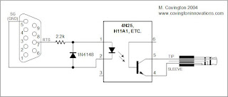

This is a pretty good scheme, but it doesn't work for my Canon EOS 400D: shutter lifting up but not going down.
After personal communications with Michael, I suspect the reason of this problem is in version of the firmware in my camera. Anyway, we have found the solution of the problem.
We have played around a bit and found the solution.

Scheme for Canon EOS 400D

After some cut-and-try iterations, we (I am and my colleague Alexey Ropyanoi) have found out why proposed scheme did not work. Now we proposing the following scheme:
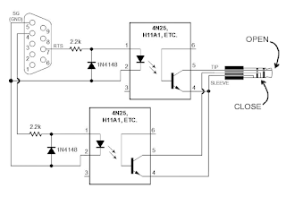
We used one more cascade to control third tip, and it works! Our laboratory Canon EOS 400D now opening and closing shutter by command from computer.

Necessary electric components
To create such remote shooting wire, you need a 4-wire cable (from audio devices or telephone cable), 2.5mm jack (or 3/32 inch jack), electrics chips mentioned above, 9-pin COM-port, and USB-COM adapter (for using this remote shooting wire on novel computers).

The best USB-COM adapter is Profilic 2303 chip: it is the most common chip and it works in Linux "out of the box".


Software
A little program on C, setSerialSignal, is required for remote control of the camera. Source code is here and it can be compiled with GCC:
gcc -o setSerialSignal setSerialSignal.c
Works on Debian GNU/Linux v4.0 r.0 "Etch", gcc version 4.1.2 20061115 (prerelease) (Debian 4.1.1-21).

This is the code:

/*
* setSerialSignal v0.1 9/13/01
* www.embeddedlinuxinterfacing.com
*
*
* The original location of this source is
* http://www.embeddedlinuxinterfacing.com/chapters/06/setSerialSignal.c
*
* This program is free software; you can redistribute it and/or modify
* it under the terms of the GNU Library General Public License as
* published by the Free Software Foundation; either version 2 of the
* License, or (at your option) any later version.
*
* This program is distributed in the hope that it will be useful, but
* WITHOUT ANY WARRANTY; without even the implied warranty of
* MERCHANTABILITY or FITNESS FOR A PARTICULAR PURPOSE. See the GNU
* Library General Public License for more details.
*
* You should have received a copy of the GNU Library General Public
* License along with this program; if not, write to the
* Free Software Foundation, Inc.,
* 59 Temple Place, Suite 330, Boston, MA 02111-1307 USA
*/
/* setSerialSignal
* setSerialSignal sets the DTR and RTS serial port control signals.
* This program queries the serial port status then sets or clears
* the DTR or RTS bits based on user supplied command line setting.
*
* setSerialSignal clears the HUPCL bit. With the HUPCL bit set,
* when you close the serial port, the Linux serial port driver
* will drop DTR (assertion level 1, negative RS-232 voltage). By
* clearing the HUPCL bit, the serial port driver leaves the
* assertion level of DTR alone when the port is closed.
*/

/*
gcc -o setSerialSignal setSerialSignal.c
*/


#include
#include
#include

/* we need a termios structure to clear the HUPCL bit */
struct termios tio;

int main(int argc, char *argv[])
{
int fd;
int status;

if (argc != 4)
{
printf("Usage: setSerialSignal port DTR RTS\n");
printf("Usage: setSerialSignal /dev/ttyS0|/dev/ttyS1 0|1 0|1\n");
exit( 1 );
}

if ((fd = open(argv[1],O_RDWR)) < 0)
{
printf("Couldn't open %s\n",argv[1]);
exit(1);
}
tcgetattr(fd, &tio); /* get the termio information */
tio.c_cflag &= ~HUPCL; /* clear the HUPCL bit */
tcsetattr(fd, TCSANOW, &tio); /* set the termio information */

ioctl(fd, TIOCMGET, &status); /* get the serial port status */

if ( argv[2][0] == '1' ) /* set the DTR line */
status &= ~TIOCM_DTR;
else
status |= TIOCM_DTR;

if ( argv[3][0] == '1' ) /* set the RTS line */
status &= ~TIOCM_RTS;
else
status |= TIOCM_RTS;

ioctl(fd, TIOCMSET, &status); /* set the serial port status */

close(fd); /* close the device file */
}


Sending signals
Compile the program setSerialSignal and make it executable. Below listed signals are described to open and close the shutter:

DTR
setSerialSignal /dev/ttyS0 1 0


Clear DTR
setSerialSignal /dev/ttyS0 0 0


RTS
setSerialSignal /dev/ttyS0 0 1


Clear RTS
setSerialSignal /dev/ttyS0 1 1


Shutter opens at DTR and closes at RTS.


Shell script for remote shooting
To automate the process of taking pictures, it is suitable to use the bash script written by Eugeni Romas aka BrainBug. Here is the modified code:


#!/bin/bash

for i in `seq $3`; do
{
setSerialSignal /dev/ttyUSB0 0 0 &&
sleep $1 && setSerialSignal /dev/ttyUSB0 0 1 &&
sleep 0.3 && setSerialSignal /dev/ttyUSB0 0 0 &&
sleep $2 && setSerialSignal /dev/ttyUSB0 1 1 && echo "One more image captured!" &&
sleep $4;

}
done

echo "Done!"


Script parameters:

1: shutter opening delay
2: exposure time, in seconds
3: amount of shots
4: delay between shots

Example:
make_captures 4 60 30 2
Script can work with USB-COM adaptor and you need to edit it if you have different port.


How does it work
Remote shooting wire is ready, inserting USB-COM adapter with wire and next:
  • Turn on the camera, set BULB mode, set aperture size and ISO speed.
  • Insert jack in the camera, another end of the wire insert in COM-USB adapter.
  • Look at dmesg log files: kernel must recognize chip and write something like this:
usb 2-1: new full speed USB device using uhci_hcd and address 2
usb 2-1: configuration #1 chosen from 1 choice
drivers/usb/serial/usb-serial.c: USB Serial support registered for pl2303
pl2303 2-1:1.0: pl2303 converter detected
usb 2-1: pl2303 converter now attached to ttyUSB0
usbcore: registered new interface driver pl2303
drivers/usb/serial/pl2303.c: Prolific PL2303 USB to serial adaptor driver
  • Now you can take pictures:
    make_capture 1 5 2 3
Here we making 2 images with 5 second exposure, the delay between shots is 3 seconds, the delay for shutter's lift 1 second.

Acknowledgements
I would like to express my gratitude to:
  • Michael A. Covington for his original article "Building a Cable Release and Serial-Port Cable for the Canon EOS 300D Digital Rebel".
  • Eugeni Romas aka BrainBug for link to the original post and discussion.
  • Anton aka NTRNO for searching key posts at Astrophorum.
  • Alexey Ropjanoi, who experimentally found out problem and eliminated it, proposing new scheme for shooting.
And I deeply thankful to my colleagues of the Solid State Physics department, Moscow Engineer Physics Institute, Russia.
Related Posts Plugin for WordPress, Blogger...